Introduction to programming microcontrollers - 2020
This is a brief introduction into programming PIC microcontrollers using MPLAB XC8 compiler.
SPI - Serial Peripheral Interface
Introduction
Serial Peripheral Interface is a bus communication that operates in full duplex mode. Devices communicate in a master/slave where the master device initializes communication. There are four pins used for SPI communication which are SDI, SCK, SDO, SS. The SDI of the master device is connected to the SDO of the slave device. Same for the SDO of the master device is connected to the SDI of the slave device.
SDI is used for incoming data from the slave device to the master, SDO is used for outgoing data from the master to slave device and SCK is the clock signal which is controlled by the master used for communicate timings. There is also a Slave Select (SS) signal which can be used for controlling multiple Slave devices which can go to a GPIO pin. Both master and slave devices should be configured for the same clock polarity for successful communication.
There are five registers for SPI mode with a PIC18F45K50 devices that need to be setting to initialize the SPI module.
- MSSP STATUS register (SSPxSTAT)
- MSSP Control register 1 (SSPxCON1)
- MSSP Control register 3 (SSPxCON3)
- MSSP Data Buffer Register (SSPxBUF)
- MSSP Address register (SSPxADD)
- MSSP Shift register (SSPxSR)
SSPxCON1 Register
| 7 | 6 | 5 | 4 | 3 | 2 | 1 | 0 |
|---|---|---|---|---|---|---|---|
| WCOL | SSPOV | SSPEN | CKP | SPM[3:0] | |||
Master Mode
- 1 = A write to SSPxBUF register was attempted resulting in collision
- 0 = No Collission
- 1 = The SSPxBUF register was written while transmitting the previous byte
- 0 = No Collision
In SPI mode:
- 1 = A new byte is received while the SSPxBUF register is still holding previous data, in this case the data in SSPxSR is lost.
- No Overflow
In both modes the corresponding pins must be properly configured as input or output.
In SPI mode:- 1 = Enables serial port and configures the associated SPI pins as the source of the serial port pins.
- 0 = Disables serial port and configures associated SPI pins as I/O port pins
CKP sets the polarity of the idle state of the clock, SPI device must have the same polarity in order to communication successfully. Where are the CKE decides on when data should be transmitted.
In SPI mode:- 1 = Idle state for clock is a high level
- 0 = Idle state for clock is a low level
These bits define the operation mode of the SPI module as well as the frequency SPI of the clock. There are more options than shown below but they are for I2C communication, so I have left those out (see the datasheet p253).
In SPI mode:- 0000 = SPI Master Mode, clock = Fosc / 4
- 0001 = SPI Master Mode, clock = Fosc / 16
- 0010 = SPI Master Mode, clock = Fosc / 64
- 0011 = SPI Master Mode, clock =TMR2 output/2
- 0100 = SPI Slave Mode, clock = SCK pin, SS pin control Enabled
- 0101 = SPI Slave Mode, clock = SCK pin, SS pin control disabled, SS can be used as I/O
- … Other values are used for the I2C protocol.
SSPxSTAT Register
| 7 | 6 | 5 | 4 | 3 | 2 | 1 | 0 |
|---|---|---|---|---|---|---|---|
| SMP | CKE | D/A | P | S | R/W | UA | BF |
In SPI mode:
- 1 = A new byte is received while the SSPxBUF register is still holding previous data, in this case the data in SSPxSR is lost.
- No Overflow
If CKP = 0
- CKE 0 = Data transmitted on falling edge of clock
- CKE 1 = Data transmitted on rising edge of clockw
- CKE 0 = Data transmitted on rising edge of clock
- CKE 1 = Data transmitted on falling edge of clock
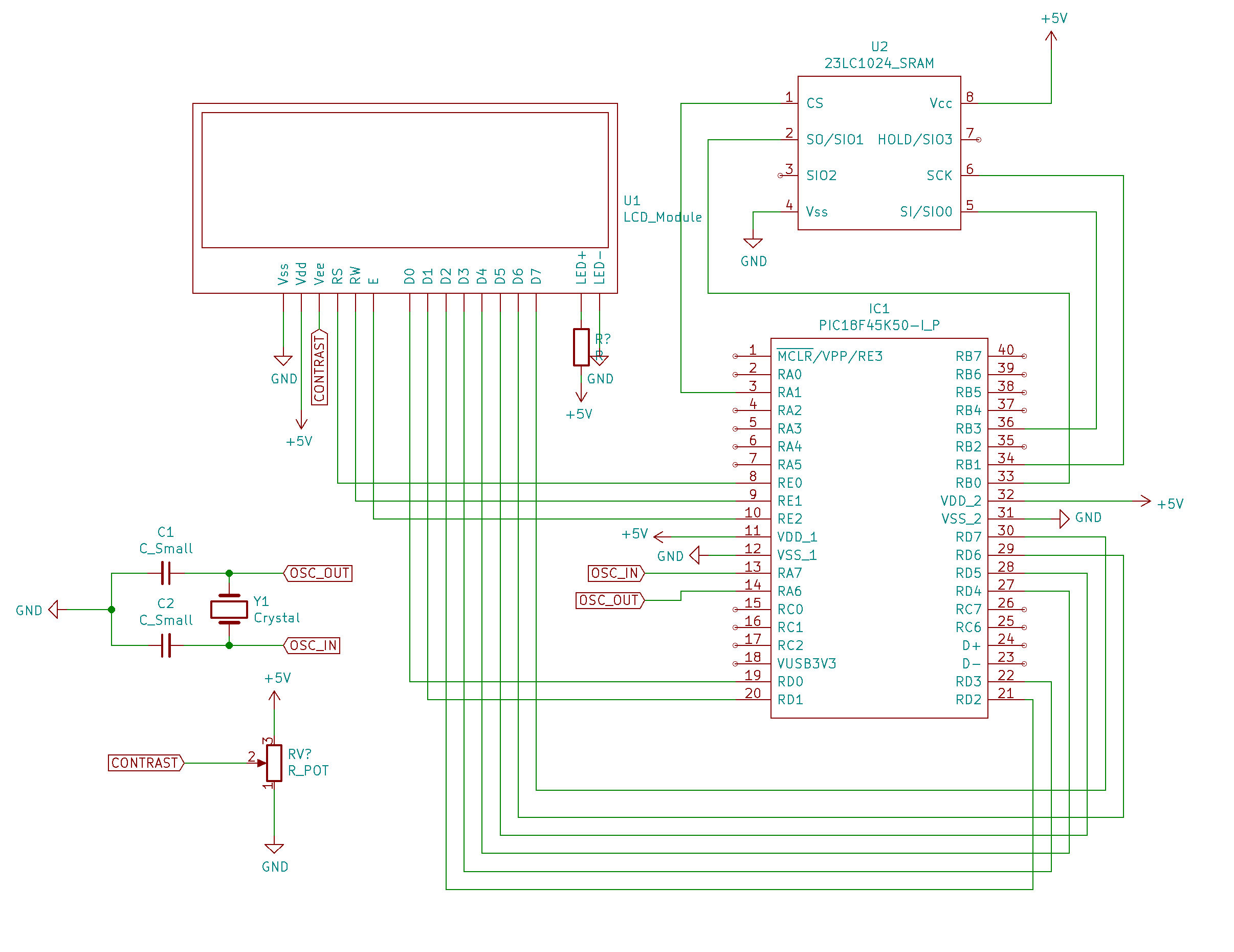
Interfacing PIC18F45K50 with SPI SRAM
This is a reference for interfacing a PIC microcontroller with a SRAM chip using SPI, specifically a 23LC1024. This SRAM chip has a 1Mbit capacity and uses SDI and SQI interfaces, with a 20Mhz clock and is can be powered using 5.0 voltage supply see datasheet for more information.
There are three operating modes available these are:
- Byte Mode - in this mode read and write operations are limited to one byte
- Page Mode - In this mode operations are limited to within the address page, the address is automatically incremented. If data reaches the page boundary then the address increments the start of the page.
- Sequential Operation - this mode allows reading and writing to the entire array, the address counter resets to 0x00000 once the operation has gone out of bounds.
Instruction Set
Instructions are sent via the SSPBUF twice, first the instruction is sent then the value for that instruction is sent through the SPI interface (SSPBUF).
| Instruction Name | Instruction Format | Hex Code | Description |
|---|---|---|---|
| READ | 0000 0011 | 0x03 | Read Data from memory starting from the selected address |
| WRITE | 0000 0010 | 0x02 | Write Data to memory starting from the selected address |
| EDIO | 0011 1011 | 0x3B | Enter Dual IO access (enter SDI bus mode) |
| EQIO | 0011 1000 | 0x38 | Enter Quad IO access (Enter SQI bus Mode) |
| RSTIO | 1111 1111 | 0xFF | Reset Dual/Quad IO access (revert to SPI bus mode) |
| RDMR | 0000 0101 | 0x05 | Read Mode Register |
| WRMR | 0000 0001 | 0x01 | Write Mode Register |
Circuit Diagram
Source Code
/*
    * File:   SRAM_23LC1024.h
    * Author: Mr Steven J Baldwin
    *
    * Created on 31 August 2020, 14:07
    */

    #ifndef SRAM_23LC1024_H
    #define SRAM_23LC1024_H

    #include <stdint.h>
    #include <xc.h>

    #define SRAM_CS         LATAbits.LA1
    #define SRAM_WRITE      0x02
    #define SRAM_READ       0x03
    #define SRAM_RDMR       0x05
    #define SRAM_WRMR       0x01
    #define SRAM_MODE_SEQU  0x40
    #define SRAM_MODE_BYTE  0x00


    #ifdef	__cplusplus
    extern "C" {
    #endif

        /**
        * SPI Functions
        */

        //   Initialize SPI module
        void SPI_init(void);

        //   Write a Byte across SPI
        void SPI_write(uint8_t data);

        //   Read a Byte across SPI
        uint8_t SPI_read();

        //   Write a 24 bit address a cross SPI MSB first
        void SPI_write_addr(uint32_t address);

        /**
        * SRAM Functions
        */

        //   Initialize SRAM module
        void SRAM_init(void);

        //   Send byte to a given address, byte operation mode.
        void SRAM_send_byte(uint32_t addr, uint8_t data);

        //   Read a byte at a given address, byte operation mode.
        uint8_t SRAM_read_byte(uint32_t addr);

        //   Send an array of bytes to store at the address given, sequence mode.
        void SRAM_send_data(uint32_t addr, void* data, uint32_t len);

        //   Read an array of bytes stored at the address given, sequence mode.
        void SRAM_read_data(uint32_t addr, void* data, uint32_t len);

        //   Which operating modes
        void SRAM_mode(uint8_t mode);


    #ifdef	__cplusplus
    }
    #endif

    #endif	/* SRAM_23LC1024_H */
/*
    * File:   SRAM.h
    * Author: Mr Steven J Baldwin
    *
    * Created on 31 August 2020, 14:07
    *
    * PIC18F45K50 - SPI SRAM (23LC1024)
    */

    #include "SRAM_23LC1024.h"
    #include "lcd_module.h"

    /*
    *
    *  Initialize Serial Peripheral Interface
    *
    */

    void SPI_init(void){

        TRISBbits.TRISB0 = 1;       //  Set SDI as input
        TRISBbits.TRISB1 = 0;       //  Set SCK as output
        TRISBbits.TRISB3 = 0;       //  Set SDO as output

        //  Set CKP low, idle state for clock is low, Enable SPI mode SSPEN
        //  Set SPI mode master, with clock = Fosc / 4 (0000)
        SSPCON1 = 0x60;

        // Set CKE high, Data transmitted on rising edge of clock
        SSPSTAT = 0x40;

        //  Clear Master Synchronous Serial Port Interrupt Flag
        PIR1bits.SSPIF = 0;

        //  Enable Master Synchronous Serial Port Interrupt
        PIE1bits.SSPIE = 1;

    }

    void SPI_write_addr(uint32_t address){

        //  Write 8 bits, bits(24-16) of address to the device
        SPI_write((address >> 16) & 0xFF);

        //  Write 8 bits, bits(16-8) of address to the device
        SPI_write((address >> 8) & 0xFF);

        //  Write 8 bits, bits(8-0) of address to the device
        SPI_write(address & 0xFF);
    }

    /**
    *  Send a Byte via the SPI and receive a byte directly after.
    *
    * @param data
    * @return
    */

    uint8_t SPI_send_receive(uint8_t data){

        SRAM_CS = 0;
        SSPBUF = data;              //  Send data to SPI buffer register
        while(!SSPSTATbits.BF);     //  Wait for transmission
        SRAM_CS = 1;                //  Set Chip select high
        while(!PIR1bits.SSPIF);     //  Wait for response
        return SSPBUF;              //  return response
    }

    /**
    *  Send a byte via the SPI to the device, ignore response
    *
    * @param data
    * @return
    */

    void SPI_write(uint8_t data){

        uint8_t data_flush;         //
        SSPBUF = data;              //  Send data to SPI buffer register
        while(!PIR1bits.SSPIF);     //  Wait for one byte transmission
        PIR1bits.SSPIF = 0;         //  Clear the flag
        data_flush = SSPBUF;        //  Ignore response

    }

    /**
    *  Receive a byte from the device via SPI
    *
    * @param data
    * @return
    */

    uint8_t SPI_read(){

        //  Flush the SSPBUF data
        SSPBUF = 0x00;
        while(!PIR1bits.SSPIF);     //  Wait for one byte transmission
        PIR1bits.SSPIF = 0;

        //  SSPBUF should contain the data sent.
        return SSPBUF;
    }

    /**
    *  Initialize Sequence for SRAM SPI device (23LC1024)
    *
    */

    void SRAM_init(void){
        SRAM_CS = 0;
        SPI_write(SRAM_RDMR);
        SPI_write(0x00);
        SRAM_CS = 1;

        SRAM_CS = 0;
        SPI_write(SRAM_WRMR);
        SPI_write(0x00);
        SRAM_CS = 1;
    }

    /**
    *  Command to change operation modes of the SRAM device (23LC1024)
    *  Mode can be either SRAM_MODE_SEQU for sequence mode or
    *  SRAM_MODE_BYTE for byte mode.
    *  To do add page operation mode...
    */

    void SRAM_mode(uint8_t mode){

        SRAM_CS = 0;                // Set Chip select low
        SPI_write(SRAM_RDMR);       // Send read operation mode command
        SPI_write(mode);            // Send new mode command
        SRAM_CS = 1;                // Set chip select high

        SRAM_CS = 0;                // Set Chip select low
        SPI_write(SRAM_WRMR);       // Send write operation mode command
        SPI_write(mode);            // Send new mode command
        SRAM_CS = 1;                // Set chip select high
    }

    uint8_t SRAM_read_byte(uint32_t addr){
        uint8_t data;
        SRAM_CS = 0;               //   Set chip select low

        SPI_write(SRAM_READ);      //   Send Write Command
        SPI_write_addr(addr);      //   Send address to read from

        data = SPI_read();         //   Read the contents of the SPI buffer register

        SRAM_CS = 1;               //   Set chip select high

        return data;
    }

    /**
    *  This is used for byte operation mode.
    *
    *  Sends one byte of data to SRAM SPI device (23LC1024)
    *  to store at the address given.
    *
    * @param addr
    * @param data
    */

    void SRAM_send_byte(uint32_t addr, uint8_t data){

        SRAM_CS = 0;                // Set Chip Select low
        SPI_write(SRAM_WRITE);      // Send Write Command
        SPI_write_addr(addr);       // Send Address to write to
        SPI_write(data);            // Send data to locate at the address
        SRAM_CS = 1;                // Set chip select high
    }

    /**
    * This is used for sequence operation mode.
    *
    * This function is used to send an array of data to SRAM SPI device (23LC1024)
    * at the address specified.
    *
    * @param addr  Address to store data
    * @param data  Data to store
    * @param len   size of data to store
    */

    void SRAM_send_data(uint32_t addr, void* data, uint32_t len)
    {
        SRAM_CS = 0;
        SPI_write(SRAM_WRITE);      //  Enter write mode
        SPI_write_addr(addr);       //  Send the start address to store the data

        uint32_t size = 0;
        uint8_t* ptr = &data[0];    //  point to buffer to send

        //  Loop through each byte
        while(size < len){
            //  Send the current byte referenced by the pointer to the device,
            //  increment the data pointer by one byte after iteration.
            SPI_write(*((uint8_t*)ptr++));

            //  increment length counter
            size++;
        }

        SRAM_CS = 1;                // Set Chip Select
    }

    /**
    *  This is used for sequence operation mode.
    *
    *  This function reads an array of data from the SRAM module, starting
    *  at the address specified.
    *
    * @param addr  Address to read data from the SRAM device(23LC1024)
    * @param data  Pointer to an array to store the received data.
    * @param len   Number of bytes to read
    */

    void SRAM_read_data(uint32_t addr, void* data, uint32_t len){

        SRAM_CS = 0;
        SPI_write(SRAM_READ);               //  Enter read operation mode
        SPI_write_addr(addr);               //  write address to the device

        uint32_t size = 0;                  //  counter

        //  pointer to array that will hold the data.
        uint8_t* ptr = (uint8_t*)data;

        //  Loop through each byte
        while(size < len){

            SSPBUF = 0x00;              //  Clear SSPBUF
            while(!PIR1bits.SSPIF);     //  Wait for one byte transmission
            PIR1bits.SSPIF = 0;         //  Clear Flag

            *ptr = SSPBUF;              //  Dereference pointer set this byte..

            ptr++;      //  Point to the next byte in the array.
            size++;     //  Increment counter
        }

        SRAM_CS = 1;    //
    }
/*
    * File:   main.c
    * Author: Mr Steven J Baldwin
    *
    * Created on 31 August 2020, 14:06
    */

    #pragma config PLLSEL = PLL4X   // PLL Selection (4x clock multiplier)
    #pragma config CFGPLLEN = OFF   // PLL Enable Configuration bit (PLL Disabled (firmware controlled))
    #pragma config CPUDIV = NOCLKDIV// CPU System Clock Postscaler (CPU uses system clock (no divide))
    #pragma config LS48MHZ = SYS24X4// Low Speed USB mode with 48 MHz system clock (System clock at 24 MHz, USB clock divider is set to 4)

    // CONFIG1H
    #pragma config FOSC = HSH   // Oscillator Selection (EC oscillator, high power 16MHz to 48MHz, clock output on OSC2)
    #pragma config PCLKEN = OFF     // Primary Oscillator Shutdown (Primary oscillator shutdown firmware controlled)
    #pragma config FCMEN = OFF      // Fail-Safe Clock Monitor (Fail-Safe Clock Monitor disabled)
    #pragma config IESO = OFF       // Internal/External Oscillator Switchover (Oscillator Switchover mode disabled)

    // CONFIG2L
    #pragma config nPWRTEN = ON     // Power-up Timer Enable (Power up timer enabled)
    #pragma config BOREN = OFF      // Brown-out Reset Enable (BOR disabled in hardware (SBOREN is ignored))
    #pragma config BORV = 285       // Brown-out Reset Voltage (BOR set to 2.85V nominal)
    #pragma config nLPBOR = ON      // Low-Power Brown-out Reset (Low-Power Brown-out Reset enabled)

    // CONFIG2H
    #pragma config WDTEN = OFF      // Watchdog Timer Enable bits (WDT disabled in hardware (SWDTEN ignored))
    #pragma config WDTPS = 1        // Watchdog Timer Postscaler (1:1)

    // CONFIG3H
    #pragma config CCP2MX = RC1     // CCP2 MUX bit (CCP2 input/output is multiplexed with RB3)
    #pragma config PBADEN = OFF     // PORTB A/D Enable bit (PORTB<5:0> pins are configured as digital I/O on Reset)
    #pragma config T3CMX = RC0      // Timer3 Clock Input MUX bit (T3CKI function is on RB5)
    #pragma config SDOMX = RB3      // SDO Output MUX bit (SDO function is on RC7)
    #pragma config MCLRE = OFF      // Master Clear Reset Pin Enable (RE3 input pin enabled; external MCLR disabled)

    // CONFIG4L
    #pragma config STVREN = OFF     // Stack Full/Underflow Reset (Stack full/underflow will not cause Reset)
    #pragma config LVP = OFF        // Single-Supply ICSP Enable bit (Single-Supply ICSP disabled)
    #pragma config ICPRT = OFF      // Dedicated In-Circuit Debug/Programming Port Enable (ICPORT disabled)
    #pragma config XINST = OFF      // Extended Instruction Set Enable bit (Instruction set extension and Indexed Addressing mode disabled)

    // CONFIG5L
    #pragma config CP0 = OFF         // Block 0 Code Protect (Block 0 is code-protected)
    #pragma config CP1 = OFF         // Block 1 Code Protect (Block 1 is code-protected)
    #pragma config CP2 = OFF         // Block 2 Code Protect (Block 2 is code-protected)
    #pragma config CP3 = OFF         // Block 3 Code Protect (Block 3 is code-protected)

    // CONFIG5H
    #pragma config CPB = OFF         // Boot Block Code Protect (Boot block is code-protected)
    #pragma config CPD = OFF         // Data EEPROM Code Protect (Data EEPROM is code-protected)

    // CONFIG6L
    #pragma config WRT0 = OFF        // Block 0 Write Protect (Block 0 (0800-1FFFh) is write-protected)
    #pragma config WRT1 = OFF        // Block 1 Write Protect (Block 1 (2000-3FFFh) is write-protected)
    #pragma config WRT2 = OFF        // Block 2 Write Protect (Block 2 (04000-5FFFh) is write-protected)
    #pragma config WRT3 = OFF        // Block 3 Write Protect (Block 3 (06000-7FFFh) is write-protected)

    // CONFIG6H
    #pragma config WRTC = OFF        // Configuration Registers Write Protect (Configuration registers (300000-3000FFh) are write-protected)
    #pragma config WRTB = OFF        // Boot Block Write Protect (Boot block (0000-7FFh) is write-protected)
    #pragma config WRTD = OFF        // Data EEPROM Write Protect (Data EEPROM is write-protected)

    // CONFIG7L
    #pragma config EBTR0 = OFF       // Block 0 Table Read Protect (Block 0 is protected from table reads executed in other blocks)
    #pragma config EBTR1 = OFF       // Block 1 Table Read Protect (Block 1 is protected from table reads executed in other blocks)
    #pragma config EBTR2 = OFF       // Block 2 Table Read Protect (Block 2 is protected from table reads executed in other blocks)
    #pragma config EBTR3 = OFF       // Block 3 Table Read Protect (Block 3 is protected from table reads executed in other blocks)

    // CONFIG7H
    #pragma config EBTRB = OFF       // Boot Block Table Read Protect (Boot block is protected from table reads executed in other blocks)

    #include <xc.h>
    #include <stdio.h>
    #include "lcd_module.h"
    #include "SRAM_23LC1024.h"

    void main(void) {

        /*
        * ANSELx registers
        */

        ANSELD = 0x00;      //  Set as digital
        ANSELC = 0x00;      //  Set as digital
        ANSELB = 0x00;      //  Set as digital
        ANSELE = 0x00;      //  Set as digital
        ANSELA = 0x00;      //  Set as digital

        ADCON1 = 0x0F;      //  Disable all Analog Inputs

        TRISA = 0x00;       //  Set Port A as output
        TRISB = 0x10;       //  Set Port B pin 0 as input, rest as output
        TRISC = 0x00;       //  Set Port C as output
        TRISD = 0x00;       //  Set Port D as output
        TRISE = 0x00;       //  Set Port E as output

        LATA = 0x00;        //  Clear Port A
        LATB = 0x00;        //  Clear Port B
        LATC = 0x00;        //  Clear Port C
        LATD = 0x00;        //  Clear Port D
        LATE = 0x00;        //  Clear Port E

        //  Initialize LCD Module
        lcd_init();

        //  Buffer to store strings
        char buf[20];

        //  Buffer to write sequence data
        uint8_t readBytes[11] = {0};

        // Display Initialized on LCD module
        sprintf(buf,"Initialized");
        lcd_send_string(buf);

        //  Delay 2 seconds
        __delay_ms(2000);

        //  Initialize SPI
        SPI_init();

        //  Initialize SRAM device
        SRAM_init();

        //  Set SRAM mode to byte operation mode
        SRAM_mode(SRAM_MODE_BYTE);

        //  Send a byte of data the number 0 to store at address 0x00.
        SRAM_send_byte(0x00, 0);

        //  Send byte array to SRAM module, using sequence mode...
        uint8_t bytes[12] = {'H', 'e', 'l','l','o', ' ', 'w','o','r','l','d',0x00};

        //  Set SRAM to sequence mode
        SRAM_mode(SRAM_MODE_SEQU);

        //  Send array to be stored at address 0x01
        SRAM_send_data(0x01, &bytes[0], 12);

        //  Execution Loop
        while(1){
            //  Clear LCD screen
            lcd_clear();

            //  Sent SRAM mode to Byte operation mode
            SRAM_mode(SRAM_MODE_BYTE);

            //  Read Byte store at address 0x00 in the SRAM device
            uint8_t byteRead = SRAM_read_byte(0x00);

            //  Increment read byte by one
            byteRead++;

            //  Store the incremented byte in the SRAM device at the same location
            SRAM_send_byte(0x00, byteRead);

            //  Read the value back
            byteRead = SRAM_read_byte(0x00);

            //  Convert the byte to a string
            sprintf(buf, "%d", byteRead);

            //  Display the value of the byte
            lcd_send_string(buf);

            //  Wait 2 seconds
            __delay_ms(2000);

            //  Set SRAM device to operating in sequence mode.
            SRAM_mode(SRAM_MODE_SEQU);

            //  Read the 11 byte sequence of character at address 0x01
            SRAM_read_data(0x01, readBytes, 12);

            // Move to the next line on the LCD module
            lcd_move_cursor(0, 1);

            // ...we could Modify the contents and write them back, this example
            // reads the contents written at the start of the program.

            //  Convert the byte array to a string
            sprintf(buf, "%s", readBytes);

            //  Display the string
            lcd_send_string(buf);

            //  Wait 2 seconds
            __delay_ms(2000);

        }
        return;
    }