Introduction to programming microcontrollers - 2020
This is a brief introduction into programming PIC microcontrollers using MPLAB XC8 compiler.
Table of Contents
Introduction to programming microcontrollers
Introduction
Programming microcontrollers requires some level of understand of low-level programming that is understanding binary, hexadecimal number system using bit wise operators. I assume that the reader of this understands either C++, C or Java programming languages. Each PIC microcontroller is different and has different GPIO count, features and specifications. Therefore you must read the datasheet of the specific controller that you are using. For demonstration purposes I am using the PIC18F45K50 which is a 40 pin DIP package that can operate at 48 Mhz.
Microcontrollers have GPIO pins that are generally accessible through CPU registers they can be configured as digital inputs or outputs. Microcontrollers generally also have specific registers for other features on the chip which may occupy the pins. Most pins can be configured as either input or output. Each pin labelled R(x)0 ~ R(x)7 are the 8 data bits, the registers LAT(x) and PORT(x) allow for writing or reading from the chip’s pins. The CPU maps registers which are a byte size to the individual pins, sending or reading binary pattern across the pins in parallel.
| Chip Pins | Rx0 | Rx1 | Rx2 | Rx3 | Rx4 | Rx5 | Rx6 | Rx7 |
|---|---|---|---|---|---|---|---|---|
| Data bits | Bit 0 | Bit 1 | Bit 2 | Bit 3 | Bit 4 | Bit 5 | Bit 6 | Bit 7 |
Example - Setting Output (43) to PORT A
| Chip Pins | Rx0 | Rx1 | Rx2 | Rx3 | Rx4 | Rx5 | Rx6 | Rx7 |
|---|---|---|---|---|---|---|---|---|
| Data bits | 0 | 0 | 1 | 0 | 1 | 0 | 1 | 1 |
LATA = 0x2B; // Decimal 43, 00101011 binary sent to PORTA registerSetting Digital Input or Output
On PIC microcontrollers this can be done using the TRIS(x) registers, a high bit of the register means that the pin is configured as input (1 for input) whereas a low is an output pin (0 for output).
Simply put in C to make all pins allocated to the PORTA register as a digital input set the register value to 0xFF or 0b11111111 or 255 decimal
TRISA = 0xFF;		//	All pins mapped to port A are now input
TRISA = 0b00000101;	//	Pins 3, and 0 are inputs all other are outputs.
TRISA = 0x00;		//	All Pins are now outputs.
To read data from a pins that are mapped to a GPIO register use the PORT(x) register.
TRISA = 0xFF;
unsigned char value;
value = PORTA;
Digital Outputs will set the corresponding pin either high or low (voltage) depending on the value of the register at the time of executing the instruction.
TRISA = 0x00;		//	All pins are digital outputs
LATA = 0xAA;		//	pins 7,5,4,2 are high the reset are low binary (1010 1010)
Circuit Diagram
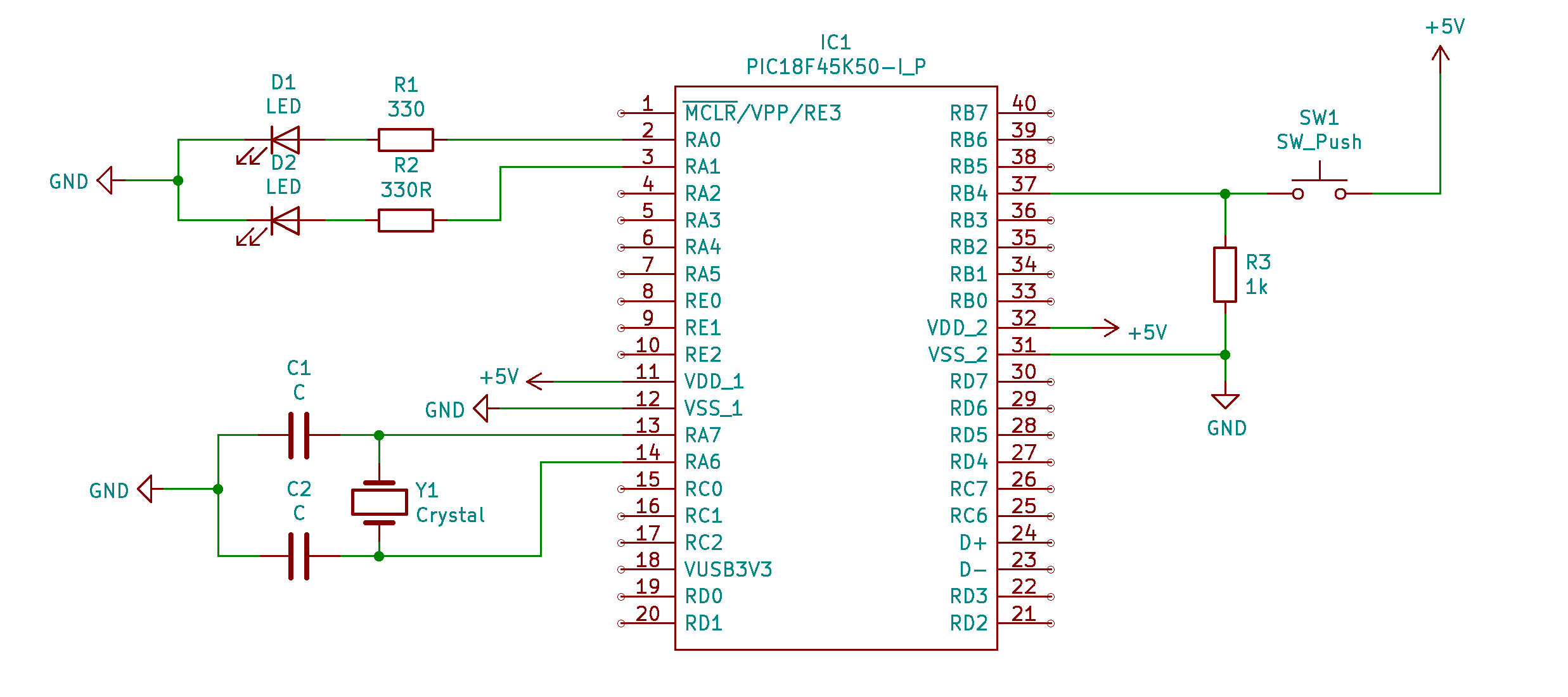
Blinking LED Example
This is a basic pic18F45k50 program that toggles a LED on and off for one second intervals. Also demonstrates inputs using interrupt on change, when this pin changes state the interrupt routine is executed which turns the LED on pin 3 on and off when released.
/*
* File:   main.c
* Author: Mr Steven J Baldwin
* Device: PIC18F45K50
* Created on 28 August 2020, 11:50
*/

// CONFIG1L
#pragma config PLLSEL = PLL4X   // PLL Selection (4x clock multiplier)
#pragma config CFGPLLEN = OFF   // PLL Enable Configuration bit (PLL Disabled (firmware controlled))
#pragma config CPUDIV = NOCLKDIV// CPU System Clock Postscaler (CPU uses system clock (no divide))
#pragma config LS48MHZ = SYS24X4// Low Speed USB mode with 48 MHz system clock (System clock at 24 MHz, USB clock divider is set to 4)

// CONFIG1H
#pragma config FOSC = LP        // Oscillator Selection (LP oscillator)
#pragma config PCLKEN = OFF     // Primary Oscillator Shutdown (Primary oscillator shutdown firmware controlled)
#pragma config FCMEN = OFF      // Fail-Safe Clock Monitor (Fail-Safe Clock Monitor disabled)
#pragma config IESO = OFF       // Internal/External Oscillator Switchover (Oscillator Switchover mode disabled)

// CONFIG2L
#pragma config nPWRTEN = ON     // Power-up Timer Enable (Power up timer enabled)
#pragma config BOREN = OFF      // Brown-out Reset Enable (BOR disabled in hardware (SBOREN is ignored))
#pragma config BORV = 285       // Brown-out Reset Voltage (BOR set to 2.85V nominal)
#pragma config nLPBOR = ON      // Low-Power Brown-out Reset (Low-Power Brown-out Reset enabled)

// CONFIG2H
#pragma config WDTEN = OFF      // Watchdog Timer Enable bits (WDT disabled in hardware (SWDTEN ignored))
#pragma config WDTPS = 1        // Watchdog Timer Postscaler (1:1)

// CONFIG3H
#pragma config CCP2MX = RB3     // CCP2 MUX bit (CCP2 input/output is multiplexed with RB3)
#pragma config PBADEN = OFF     // PORTB A/D Enable bit (PORTB<5:0> pins are configured as digital I/O on Reset)
#pragma config T3CMX = RB5      // Timer3 Clock Input MUX bit (T3CKI function is on RB5)
#pragma config SDOMX = RC7      // SDO Output MUX bit (SDO function is on RC7)
#pragma config MCLRE = OFF      // Master Clear Reset Pin Enable (RE3 input pin enabled; external MCLR disabled)

// CONFIG4L
#pragma config STVREN = OFF     // Stack Full/Underflow Reset (Stack full/underflow will not cause Reset)
#pragma config LVP = OFF        // Single-Supply ICSP Enable bit (Single-Supply ICSP disabled)
#pragma config ICPRT = OFF      // Dedicated In-Circuit Debug/Programming Port Enable (ICPORT disabled)
#pragma config XINST = OFF      // Extended Instruction Set Enable bit (Instruction set extension and Indexed Addressing mode disabled)

// CONFIG5L
#pragma config CP0 = ON         // Block 0 Code Protect (Block 0 is code-protected)
#pragma config CP1 = ON         // Block 1 Code Protect (Block 1 is code-protected)
#pragma config CP2 = ON         // Block 2 Code Protect (Block 2 is code-protected)
#pragma config CP3 = ON         // Block 3 Code Protect (Block 3 is code-protected)

// CONFIG5H
#pragma config CPB = ON         // Boot Block Code Protect (Boot block is code-protected)
#pragma config CPD = ON         // Data EEPROM Code Protect (Data EEPROM is code-protected)

// CONFIG6L
#pragma config WRT0 = ON        // Block 0 Write Protect (Block 0 (0800-1FFFh) is write-protected)
#pragma config WRT1 = ON        // Block 1 Write Protect (Block 1 (2000-3FFFh) is write-protected)
#pragma config WRT2 = ON        // Block 2 Write Protect (Block 2 (04000-5FFFh) is write-protected)
#pragma config WRT3 = ON        // Block 3 Write Protect (Block 3 (06000-7FFFh) is write-protected)

// CONFIG6H
#pragma config WRTC = ON        // Configuration Registers Write Protect (Configuration registers (300000-3000FFh) are write-protected)
#pragma config WRTB = ON        // Boot Block Write Protect (Boot block (0000-7FFh) is write-protected)
#pragma config WRTD = ON        // Data EEPROM Write Protect (Data EEPROM is write-protected)

// CONFIG7L
#pragma config EBTR0 = ON       // Block 0 Table Read Protect (Block 0 is protected from table reads executed in other blocks)
#pragma config EBTR1 = ON       // Block 1 Table Read Protect (Block 1 is protected from table reads executed in other blocks)
#pragma config EBTR2 = ON       // Block 2 Table Read Protect (Block 2 is protected from table reads executed in other blocks)
#pragma config EBTR3 = ON       // Block 3 Table Read Protect (Block 3 is protected from table reads executed in other blocks)

// CONFIG7H
#pragma config EBTRB = ON       // Boot Block Table Read Protect (Boot block is protected from table reads executed in other blocks)

// #pragma config statements should precede project file includes.
// Use project enums instead of #define for ON and OFF.

#include <xc.h>

//Crystal Frequency in herz (20Mhz) this macro used for the xc8 __delay functions.
#define _XTAL_FREQ 20000000

/**
*  Interrupt Routine executed when interrupt occurs
*
*/

void __interrupt(high_priority) interrup_isr(void){
    unsigned char tmp;

    //  Check for Interrupt on change flag
    if(INTCONbits.IOCIF == 1){
        tmp = PORTB;                    //  Read PortB
        LATAbits.LA1 = ~LATAbits.LA1;   //  Toggle LED on pin 3 (RA1)
        INTCONbits.IOCIF = 0;           //  Clear the interrupt on change flag
    }

    INTCONbits.IOCIF = 0;
    INTCONbits.INT0IF = 0;
}

/**
*
*  Main program routine
*
*/

void main(void) {

    /*
    * ANSELx registers
    */

    ANSELD = 0x00;      //  Set as digital
    ANSELC = 0x00;      //  Set as digital
    ANSELB = 0x00;      //  Set as digital
    ANSELE = 0x00;      //  Set as digital
    ANSELA = 0x00;      //  Set as digital

    ADCON1 = 0x0F;      //  Disable all Analog Inputs

    TRISA = 0x00;       //  Set Port A as output
    TRISB = 0x10;       //  Set Port B pin RB4 as input, rest as output
    TRISC = 0x00;       //  Set Port C as output
    TRISD = 0x00;       //  Set Port D as output
    TRISE = 0x00;       //  Set Port E as output

    LATA = 0x00;        //  Clear Port A
    LATB = 0x00;        //  Clear Port B
    LATC = 0x00;        //  Clear Port C
    LATD = 0x00;        //  Clear Port D
    LATE = 0x00;        //  Clear Port E

    IOCBbits.IOCB4 = 1;     //  Enable Interrupt On Change Pin (37 - ICOB3)

    INTCONbits.IOCIE = 1;   //  Enable Interrupt On Change
    INTCONbits.PEIE = 1;    //  Enable Peripheral Interrupts
    INTCONbits.GIE=1;       //  Enable Global Interrupts

    //  Execution Loop
    while(1){

        __delay_ms(1000);               //  Wait 1 second
        LATAbits.LA0 = ~LATAbits.LA0;   //  Toggle pin 2 (RA0)

        __delay_ms(1000);               //  Wait 1 second
        LATAbits.LA0 = ~LATAbits.LA0;   //  Toggle pin 2 (RA0)
    }

    return;
}